Miscellaneous
Direct Memory Access (DMA) Modes
DMA Modes and Configuration for DAC Sine Wave Output
DMA Transfer Modes
-
Normal Mode:
The DMA controller performs a single transfer (or a fixed number of transfers) and then stops. You must manually re-enable it for the next transfer.
Not ideal for continuous signals like a sine wave. -
Circular Mode:
After reaching the end of the buffer, the DMA automatically wraps around to the beginning and continues transferring.
Best for generating continuous waveforms with DAC (e.g., sine wave) or reading constant ADC, as the DMA endlessly loops through your pre-calculated table without CPU intervention.
Address Increment Settings
- Peripheral Increment Address:
- What it does: Determines if the peripheral’s address register (e.g., the DAC data register) should be incremented after each transfer.
- Setting: Disable
- Why: The DAC data register is always at a fixed address; the DMA should always write to the same place.
- Memory Increment Address:
- What it does: Determines if the memory address (your sine wave table in RAM) should be incremented after each transfer.
- Setting: Enable
- Why: This allows the DMA to step through each value in your sine wave data array.
Data Direction
- Memory to Peripheral:
- Data moves from your memory buffer (f.ex in out DAC-Sine wave generation example, sine wave array) to the peripheral (DAC register).
- Setting: Memory to Peripheral
- Why: This is the only direction that makes sense for feeding data from your sine wave table to the DAC.
Data Width
- Byte (8-bit): Transfers 1 byte at a time
- Half Word (16-bit): Transfers 2 bytes at a time
- Word (32-bit): Transfers 4 bytes at a time
The STM32F767 DAC is a 12-bit converter, but it can be accessed in 16-bit or 32-bit format.
To match the DAC_ALIGN_12B_R alignment used with HAL_DAC_SetValue, choose Half Word (16-bit) data width. This matches the format used by the HAL library.
Summary Table: Ideal DMA Settings for Continuous Sine Wave Output
| Setting | Value |
|---|---|
| Mode | Circular |
| Peripheral Increment | Disable |
| Memory Increment | Enable |
| Direction | Memory to Peripheral |
| Data Width | Half Word (16-bit) |
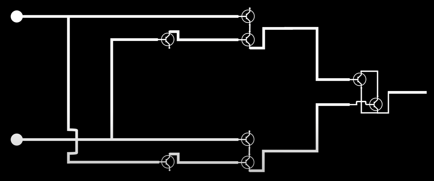
What does it really mean that everything consists of transistors?
We have agreed on that everything is ones and zeros. All the process in a digital system is about moving ones and zeros from one memory, but how electronically are they stored?
Memory is about how to retain information.
How do transistors run code? How do transistors remember data?
Power of abstraction! Source
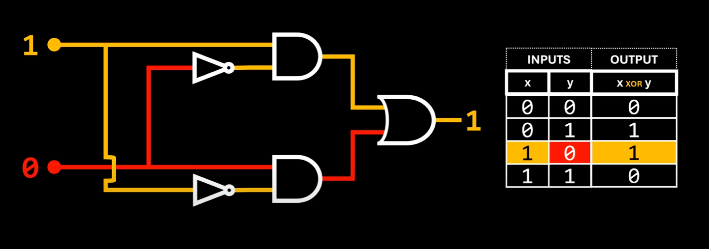
By using different gates, we create amazingly beautiful and useful circuits to process the data or signal. One of the most fundamental circuits for a digital system is an adder.
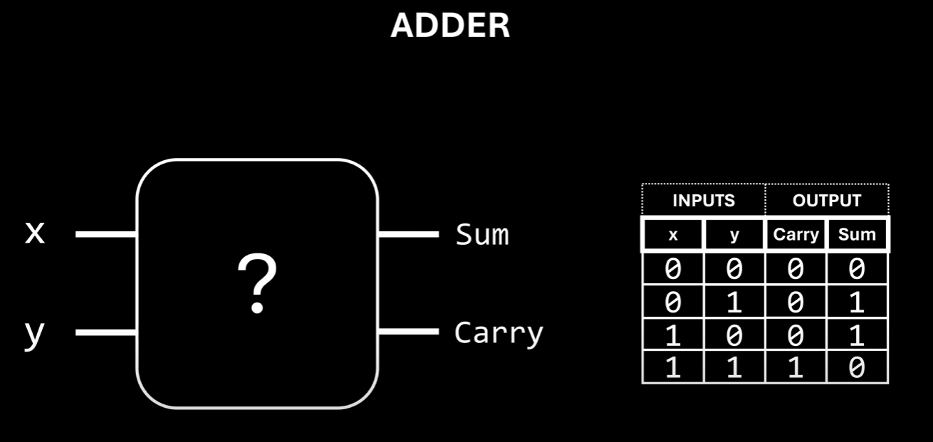
An adder is a digital circuit that performs addition of numbers. In its simplest form, a half-adder can add two single binary digits and produce a sum and a carry value. A full-adder extends this by also taking into account a carry input, allowing us to chain multiple adders together to add multi-bit binary numbers, which is essential for arithmetic operations in computers.
Adders are not only used for arithmetic, but also form the basis for more complex operations such as subtraction, multiplication, and even logical operations. In fact, the arithmetic logic unit (ALU) of a microprocessor is built from a combination of adders and other logic gates. The efficiency and speed of these basic circuits directly impact the performance and power consumption of the entire system.
Understanding how these gates and circuits are constructed from transistors helps us appreciate the physical limitations and trade-offs in digital design. For example, more complex circuits require more transistors, which means more power consumption and more space on the chip. This is why, in embedded systems, we often need to carefully consider how much memory and processing power we actually need, and optimize our designs accordingly.
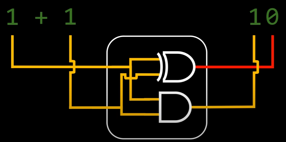 As you see, you can combine an XOR gate and an AND gate, and create a simple, instantaneous adder.
I think this is where the beauty of an embedded system lies. Simple and fast. Unlike programming on a general-purpose operating system, where layers of abstraction and resource management often hide the underlying hardware, embedded system design puts you in direct contact with the physical world. Every line of code you write can have a tangible effect on power consumption, speed, and reliability.
On an operating system, you might not worry about how memory is allocated. There’s usually plenty of resources, and the OS handles much of the complexity for you. However in embedded systems, you are both the architect and the craftsman: you must carefully choose what to include, optimize for every byte and every microamp, and understand the hardware intimately. This directness is both a challenge and a joy. You get to see the immediate results of your optimizations; an LED blinks faster, a sensor uses less power, a device runs longer on a battery. The constraints force you to be creative and efficient.
Anyways, let’s cut the praise and continue the actual business.
STM32F767ZI Nucleo-144 Default Pin Assignments
When creating a project for the STM32F767ZI Nucleo-144 board in STM32CubeMX, the following pins are configured by default to support essential on-board features, debugging, and clocking.
1. System and Clock Configuration (RCC)
These pins are connected to the external crystal oscillators on the Nucleo board.
| Pin | Peripheral | Function | Explanation |
|---|---|---|---|
| PH0 | RCC_OSC_IN |
High-Speed External (HSE) Input | Main system clock input (typically 8 MHz crystal). |
| PH1 | RCC_OSC_OUT |
High-Speed External (HSE) Output | Main system clock output. |
| PC14 | RCC_OSC32_IN |
Low-Speed External (LSE) Input | Clock input for the RTC (Real-Time Clock) (32.768 kHz crystal). |
| PC15 | RCC_OSC32_OUT |
Low-Speed External (LSE) Output | Clock output for the RTC. |
2. Debugging and Programming (SWD)
These pins are dedicated to the on-board ST-LINK/V2-1 debugger/programmer.
| Pin | Peripheral | Function | Explanation |
|---|---|---|---|
| PA13 | SYS_JTMS-SWDIO |
Serial Wire Debug Data (SWDIO) | Data I/O line for programming and debugging. |
| PA14 | SYS_JTCK-SWCLK |
Serial Wire Debug Clock (SWCLK) | Clock line for the SWD interface. |
3. On-Board Peripherals (LEDs and Button)
These pins connect to the user-interface components on the Nucleo-144 board.
| Pin | Peripheral | Board Label | Function |
|---|---|---|---|
| PC13 | GPIO_Input |
USER_Btn (B1) | User Push Button. Configured as input. |
| PB0 | GPIO_Output |
LD1 (Green) | User-programmable LED. |
| PB7 | GPIO_Output |
LD2 (Blue) | User-programmable LED. |
| PB14 | GPIO_Output |
LD3 (Red) | User-programmable LED. |
4. Virtual COM Port (VCP)
The ST-LINK is typically wired to the USART3 peripheral to create a VCP over USB for serial terminal communication.
| Pin | Peripheral | Function |
|---|---|---|
| PD8 | USART3_TX |
Transmit for Virtual COM Port |
| PD9 | USART3_RX |
Receive for Virtual COM Port |
5. Ethernet (RMII Interface)
The STM32F767ZI Nucleo-144 features an Ethernet PHY, typically configured using the RMII (Reduced Media Independent Interface). A PHY is an abbreviation for the Physical Layer (Layer 1) of the OSI networking model, or more commonly, it refers to the PHY chip (or transceiver) that implements this layer’s functions.
| Pin | Peripheral | Function |
|---|---|---|
| PA1 | RMII_REF_CLK |
Reference Clock (50 MHz) |
| PA7 | RMII_CRS_DV |
Carrier Sense / Data Valid |
| PB11 | RMII_TX_EN |
Transmit Enable |
| PB12 | RMII_TXD0 |
Transmit Data 0 |
| PB13 | RMII_TXD1 |
Transmit Data 1 |
| PC4 | RMII_RXD0 |
Receive Data 0 |
| PC5 | RMII_RXD1 |
Receive Data 1 |
| PC1 | ETH_MDC |
Management Data Clock |
| PA2 | ETH_MDIO |
Management Data I/O |
6. USB OTG High Speed (HS)
USB On-The-Go (OTG) is a specification that allows portable USB devices to be cabled together without a computer. When using the standard USB protocol, one device, most commonly a computer, will always be the host, and the other device will always be the peripheral. With a USB OTG cable, both devices can act as either a host or peripheral, allowing for interaction between two traditionally peripheral devices. (Source:totalphase.com) The board’s USB Type B connector for High-Speed communication is wired to the USB OTG HS peripheral, often using a ULPI (UTMI+ Low Pin Interface) PHY.
| Pin | Peripheral | Function |
|---|---|---|
| PA5 | USB_OTG_HS_ULPI_CK |
ULPI Clock |
| PB0 | USB_OTG_HS_ULPI_D1 |
ULPI Data 1 |
| PB1 | USB_OTG_HS_ULPI_D2 |
ULPI Data 2 |
| PB10 | USB_OTG_HS_ULPI_D3 |
ULPI Data 3 |
| PB11 | USB_OTG_HS_ULPI_D4 |
ULPI Data 4 |
| PB12 | USB_OTG_HS_ULPI_D5 |
ULPI Data 5 |
| PB13 | USB_OTG_HS_ULPI_D6 |
ULPI Data 6 |
| PC0 | USB_OTG_HS_ULPI_STP |
ULPI Stop |
| PC2 | USB_OTG_HS_ULPI_DIR |
ULPI Direction |
7. Power and Ground Pins (Unlabeled when you start)
While not explicitly highlighted with a peripheral name, many pins on the periphery of the chip are dedicated to power, ground, and analog reference:
- VDD / VSS: Power supply (3.3V) and Ground for the digital core.
- VCA / VSA: Power supply and Ground for the analog components (like ADC/DAC).
- VBAT: Power supply for the RTC and backup registers.
- VREF+ / VREF-: Reference voltages for the Analog-to-Digital Converter (ADC) and Digital-to-Analog Converter (DAC).
- BOOTO: Boot mode selection pin (used to select boot from main Flash, System memory, or SRAM).