Lecture 5 - ADC (Analog-to-Digital Conversion
ADC (Analog to Digital Conversion)
Analog to digital converters (ADC) and digital to analog converters (DAC) are the bridges between digital and analog worlds.
The analog to digital converter has many applications, some of which include:
- Reading of potentiometer settings
- Reading of temperature sensors, pressure sensors, light sensors, strain sensors, etc.
- Reading the voltage on a battery in order to determine the state of charge (sometimes combined with a temperature reading, since battery voltage can be affected by temperature)
- Measurement of EMF in order to determine the rotational speed of a motor
- Measurement of voltage and current in power systems in order to calculate active (P), and reactive (Q) power
- Reception of radio signals for use in a software defined radio (SDR)
Analog to digital converter
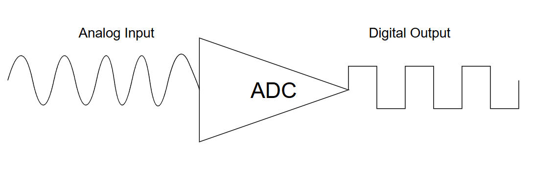
An A/D converter (analog to digital converter) is a device that converts a analog signal into an approximate digital representation. It measures the ratio of an analog input value to a reference value and express it in a form of digital value. Many different technologies exists for this purpose, where each one has it’s own advantages and disadvantages.
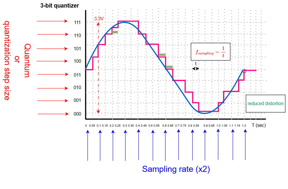
The simplest A/D converter is a bunch of comparator circuits. In the figure below, you see a 3-bit A/D converter.
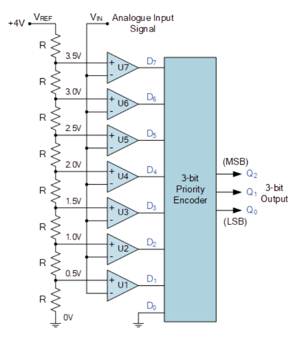 Source:www.electronics-tutorials.ws/
Did you realize that the whole analog signal range is divided into 8 possibilities? You can increase it, but it will cost you more, so being optimal in design is the key.
Real-world ADC
Language is discrete, feelings are not
One may think about this analog-digital trade off as an art of categorization. When I say everything in this world is continuous, I mean it. Let’s do a bit psychological brainstorming, shall we? Think about your feelings. When you experience something that makes you happy, you describe/express it with a word: Happy. What if you are really happy? Well, you can emphasize your word (very happy) or categorize and redefine your happiness with another word: Amused. If that’s not enough, you can always increase your precision: (very amused) or thrilled.
What is important in here is not the language but the limitation of the language (which has a discrete characteristic) when you want to express your feelings (which have a continuous characteristic). It is never the exact representation of what you really feel when you speak it out. This leads me to the conclusion that you will always lose when you trade off between analog and digital.
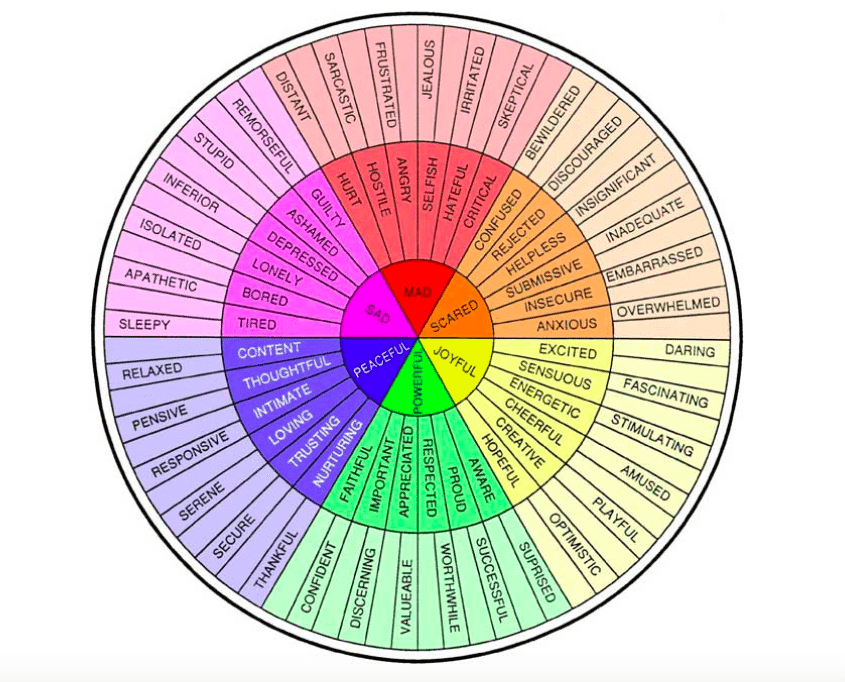
Digital to Analog Conversion of feelings. The language is discrete. Source:www.simplemost.com
So, you can think about expressing your feelings with words as ANALOG-TO-DIGITAL conversion. Understanding what someone feel when they told you as DIGITAL-TO-ANALOG conversion.
Quantization
Quantization is the main step in digitizing an analog signal. Basically, categorize an analog signal into subset of digital values which can be expressed in desired resolution. Let’s have a look at a quantized sinusoidal signal in 4-bits resolution.
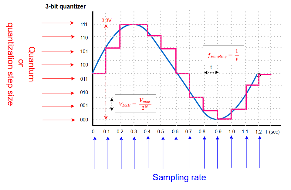
- Sampling depth is the minimum smallest analog value change that is detectable.
- Sampling rate is the number of samples taken for quantization.
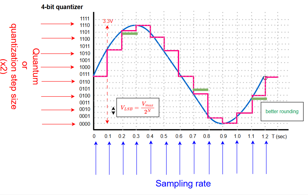
Note that as we discussed before that we cannot every possible analog output in digital world (as we encounter conversion error), we cannot measure every possible analog input with an infinite precision, either. ADC is used a lot in audio production. If you want to have a more intuitive explanation of ADC, resolution, samling frequency and quantization, please watch this video
Question:Considering the fact that your reference analog voltage is 5V and you are using 10-bit ADC converter, what is the minimum analog voltage difference you can distinguish? Answer: 4.9mv
Question:Do you think if there is any limitation of how fast/slow you can sample a signal? What is the advantages and disadvantages of sampling fast/slow? Answer: Yes. See more: Aliasing
Important parameters for ADC operation
There are many important parameters one should understand when applying an A/D converter. Even if a particular ADC is selected, there are still many parameters that can be adjusted within the ADC depending on how you intend to use it. The following is a summary of a few basic ones:
- Analog Input (V_in): The continuous voltage signal you want to convert.
- Digital Output (D_out): The discrete numerical value representing the analog input.
- Resolution: The number of bits used to represent the analog signal digitally. This determines the smallest possible change in the analog value that the converter can detect. For example, a 12-bit ADC can represent \(2^{12} = 4096\) distinct levels.
- Sampling frequency: The rate at which the analog signal is sampled and converted to digital. This limits how quickly changes in the analog signal can be detected.
- Aliasing: If the analog signal contains frequency components higher than half the sampling frequency, aliasing can occur. This means the digital output may contain frequency components not present in the original analog signal.
- Reference Voltage (V_ref): This is the maximum voltage the ADC can measure. The digital output is a fraction of this reference voltage. For example, if V_ref is 3.3V and you have a 12-bit ADC, each step represents \(3.3V/4096 \approxeq 0.8mV\).
- Channels: ADCs often have multiple input channels, allowing you to connect several analog sensors to a single ADC module.
For simple applications with slowly varying values (e.g., temperature measurements), considering just these parameters may be sufficient. For more demanding applications (e.g., real-time current measurements in a motor drive), a deeper understanding of all parameters affecting ADC performance is necessary.
The analog input or output range is determined by a reference voltage, \(V_{ref}\). Typically for an N-bit converter with unsigned digital I/O and unipolar analog range \((0V .. +V_{ref})\), one step at the analog end, \(\Delta V_{LSB}\), is given by:
\[\Delta V_{LSB} = \frac{V_{ref}}{2^N}\]where LSB stands for Least Significant Bit. Similarly for a bipolar analog range \((-V_{ref} .. +V_{ref})\), one step at the analog end is:
\[\Delta V_{LSB} = \frac{V_{ref+} - V_{ref-}}{2^N}\]Another important thing is that the ADC is super slow process in 108 Mhz (about 9.26 ns) levels. For comparison, HAL_GPIO_TogglePin() takes around 50ns whereas HAL_ADC_Start() + HAL_ADC_GetValue() 500ns! We can reduce the sampling times, lower the resolution and can use DMA(Direct Memory Access) etc. to make it faster. For now, we keep the ADC in our main process but there are other ways to optimize your program when you need to include such a bulky process in your applications. Just DO NOT FORGET THAT ADC IS A BULKY PROCESS AND HALTS YOUR SYSTEM WITH THE DEFAULT SETTINGS.
Using ADC in STM32F767
In the reference manual in section-15, you will find how to use ADC and the properties of the A/D converter in our microcontroller.
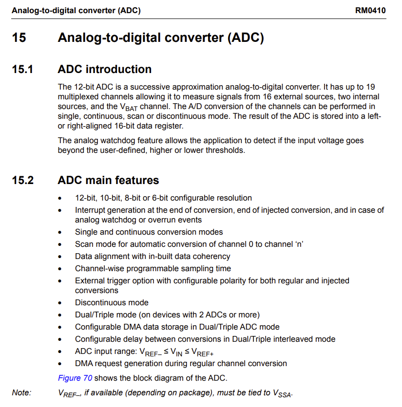
ADC input pins are generally designated as ADCx_INy, where x is the ADC module number (1, 2, or 3) and y is the channel number.
HAL Functions for ADC
The STM32Cube HAL (Hardware Abstraction Layer) provides a set of user-friendly functions to configure and manage the ADC peripheral. Here are some of the most commonly used ones:
HAL_ADC_Init(ADC_HandleTypeDef* hadc): Initializes the ADC peripheral with the specified parameters inhadc. This function is typically generated by CubeMX.HAL_ADC_ConfigChannel(ADC_HandleTypeDef* hadc, ADC_ChannelConfTypeDef* sConfig): Configures a specific ADC channel with parameters like channel number, rank (for scan mode), and sampling time. Also typically generated by CubeMX.HAL_ADC_Start(ADC_HandleTypeDef* hadc): Starts ADC conversion in polling mode.HAL_ADC_PollForConversion(ADC_HandleTypeDef* hadc, uint32_t Timeout): Waits for an ADC conversion to complete in polling mode. ReturnsHAL_OKif successful within the timeout period.HAL_ADC_GetValue(ADC_HandleTypeDef* hadc): Retrieves the converted digital value from the ADC data register.HAL_ADC_Start_IT(ADC_HandleTypeDef* hadc): Starts ADC conversion in interrupt mode.HAL_ADC_Start_DMA(ADC_HandleTypeDef* hadc, uint32_t* pData, uint32_t Length): Starts ADC conversion in DMA mode.pDatais the pointer to the destination buffer, andLengthis the number of conversions.HAL_ADC_Stop_IT(ADC_HandleTypeDef* hadc): Stops ADC conversion in interrupt mode.HAL_ADC_Stop_DMA(ADC_HandleTypeDef* hadc): Stops ADC conversion in DMA mode.HAL_ADC_ConvCpltCallback(ADC_HandleTypeDef* hadc): A weak callback function that gets called automatically by the HAL driver when an ADC conversion (or sequence of conversions in scan mode) completes in interrupt or DMA mode. You should override this in yourmain.cor another source file to implement your custom logic.HAL_ADC_ErrorCallback(ADC_HandleTypeDef* hadc): A weak callback function that gets called when an ADC error occurs.
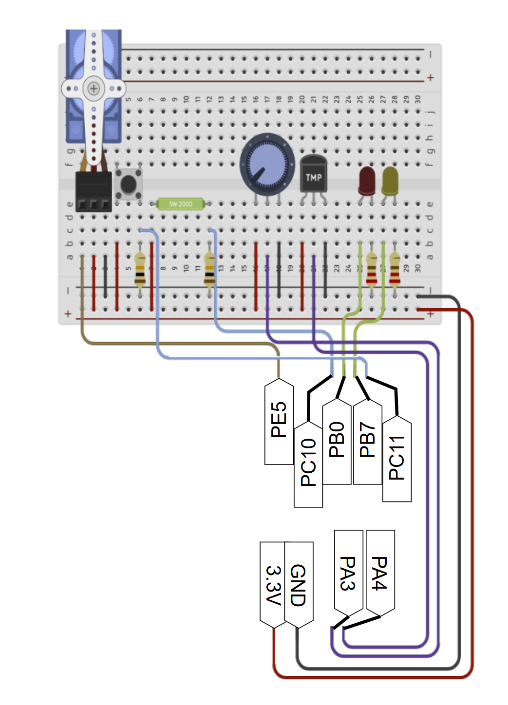
A common circuit
A common circuit for almost all exercises for a few weeks.
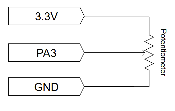
Exercise: Read potentiometer value
In this exercise, we will read the value of a potentiometer and convert it into voltage. It is a fundamental step to be able to read many different sensors later on.
- Connect your potentiometer as shown in the figure.
- Create a new project without default mode and connect ceramic/crystal resonator on the
System Core > RCC > HSE. - Find
PA3on the chip and set it toADC1_IN3. Change the label toPOT_IN. - At this step, we will change only the
ADC Regular Converion Mode > Rank > Sampling Timein the ADC setup. This will allow to adjust the duration the input voltage is held on the sampling capacitor before conversion. This is crucial for optimizing both conversion speed and accuracy. We keep the rest the same for now to see how efficient it is with the default settings.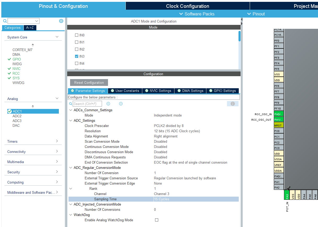
- Do the same clock configurations: 8Mhz input frequency and 108 Mhz HCLK. Resolve Clock issues.
- Give a proper name to your project. Do the necessary changes and generate your code.
- Create a platformio.ini with this content:
[env:nucleo_f767zi] platform = ststm32 board = nucleo_f767zi framework = stm32cube build_flags = -IInc upload_protocol = stlink debug_tool = stlink debug_build_flags = -O0 -g -ggdb - Define necessary variables in
main.cafter/* USER CODE BEGIN 1 */:uint32_t adc_value = 0; float voltage = 0.0; - Do the ADC work. Place this code after
/* USER CODE BEGIN 3 */:HAL_ADC_Start(&hadc1); // Start ADC conversion HAL_ADC_PollForConversion(&hadc1, HAL_MAX_DELAY); // Wait for conversion to complete adc_value = HAL_ADC_GetValue(&hadc1); // Get the converted value // Convert ADC value to voltage // V_ref is 3.3V and 12-bit resolution (4096 levels) voltage = (float)adc_value * (3.3f / 4095.0f); HAL_Delay(100); // Small delay - Build and upload.
- Open the debugger and add both
adc_valueandvoltageto your watch list. You can add a breakpoint at theHAL_ADC_Start. - Observe that
voltagechanges between 0-3.3V andadc_valuechanges between 0-4095.
Exercise (Home/Lab): Auto turn on/off LED on with LDR
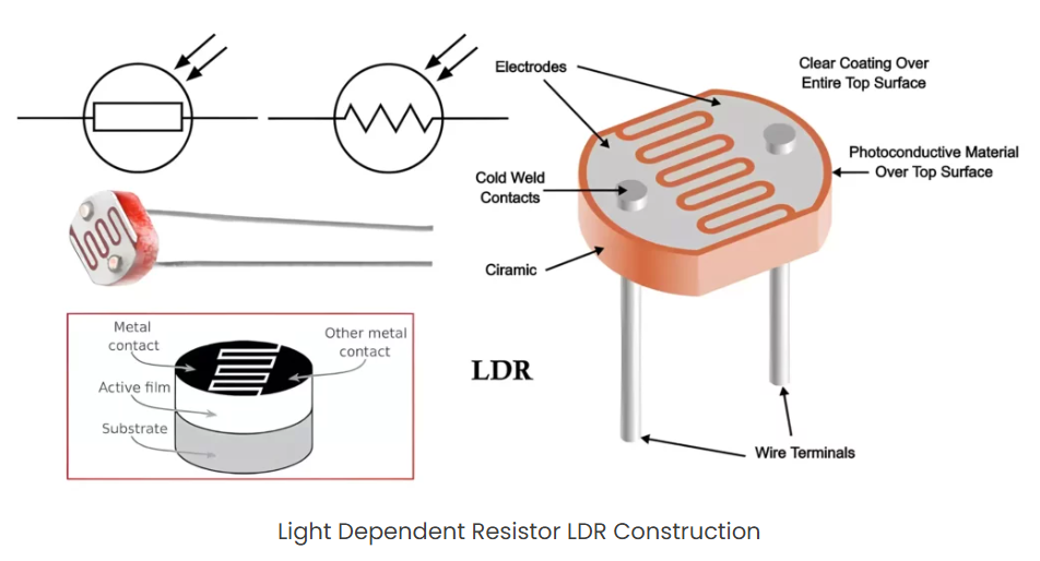
LDRs (Light Dependent Resistors) are commonly used in devices like automatic streetlights, light meters, security systems, and even in some types of audio compressors. Their resistance decreases with increasing light intensity, allowing them to be used as light sensors.
 Source:hackatronic.com
You will connect it to your mictocontoller like this:
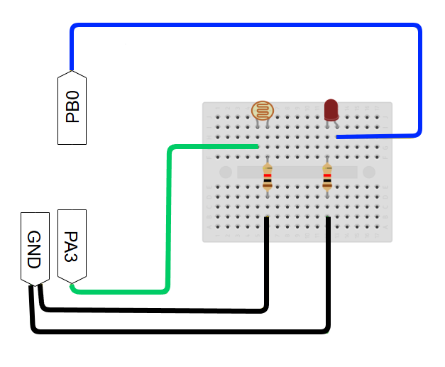
Most of the simple analog sensors (temperature sensor, humidity sensor, force sensor etc.) work in the same principle. If you are missing a component, you can use another 2-legged analog sensor. If you don’t have anything that can be used instead of LDR, talk to your lecturer. S/he will provide it to you.
Exercise: Measure A/D conversion duration
In this exercise, we will combine timers and ADC concept and measure how much it takes to finish the A/D conversion. The main purpose is to see that ADC is a blocking event and with the current settings, you are not able much until the ADC is done with the current settings.
To start, you can either do changes on your previous project or create a new one and do the necessary pinout & clock configurations. I will explain the steps related to the timer here.
- We will use
TIM3for this exercise just because it is a general-purpose timer. We could use another timer but we MUST BE CAREFUL in choosing the timer to measure time. If you check the datasheet, you see thatPA3can serve several purposes and it is connected toTIM2_CH4,TIM5_CH4andTIM9_CH2. You must avoid using those channels, but it is easier to avoid those timers in this exercise altogether not to cause any conflicts.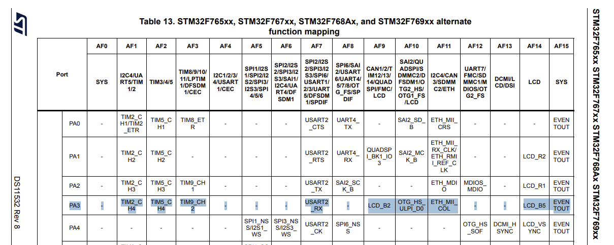
- Select Internal Clock for the Clock Source and set the prescalar to 108-1. Therefore our 1 tick will take 1us since our HCLK os set to 108 Mhz. We don’t need to generate interrupt or set a pin as input or output. We just want to measure time. Simple. The
TIM3settings should look like this: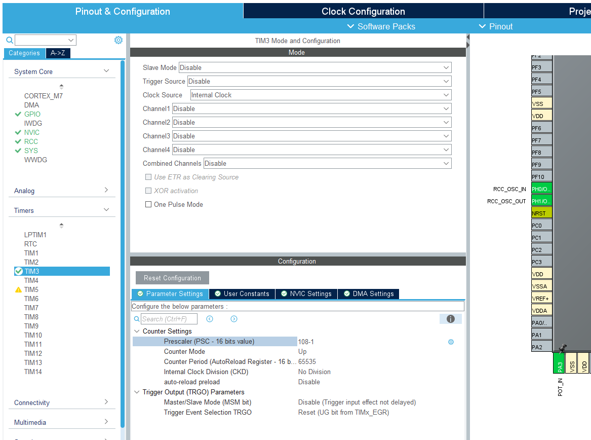
- Give a proper name to your project. Do the necessary changes and generate your code.
- Create a platformio.ini with the previous content.
- Update the necessary variables in
main.cafter/* USER CODE BEGIN 1 */:uint32_t adc_value = 0; float voltage = 0.0; uint32_t start_time = 0; uint32_t end_time = 0; uint32_t conversion_duration_us = 0; - Start the timer before the infinite loop starts. Place this after
/* USER CODE BEGIN 2 */:HAL_TIM_Base_Start(&htim3); // Start the timer -
Update the code after
/* USER CODE BEGIN 3 */:start_time = __HAL_TIM_GET_COUNTER(&htim3); // Get current timer value // Our ADC conversion starts HAL_ADC_Start(&hadc1); HAL_ADC_PollForConversion(&hadc1, HAL_MAX_DELAY); adc_value = HAL_ADC_GetValue(&hadc1); // Our ADC conversion ends end_time = __HAL_TIM_GET_COUNTER(&htim3); // Get timer value after conversion // Calculate duration, handling potential timer overflow (for simplicity, assuming no overflow within conversion time) if (end_time >= start_time) { conversion_duration_us = end_time - start_time; } else { // Handle timer overflow if conversion takes longer than timer period (unlikely for single ADC conv) conversion_duration_us = (65535 - start_time) + end_time; // For a 16-bit timer } voltage = (float)adc_value * (3.3f / 4095.0f); HAL_Delay(500); - Build and upload.
- Observe
conversion_duration_usin debugger’s watchlist. It will be in the order of microseconds.
You will see that conversion_duration_us value fluctuates a lot. Especially when trying to measure very short durations (~500ns) with polling methods and system overhead. It’s not necessarily that the ADC conversion itself is unreliable, but rather that your measurement method is picking up noise from other CPU activities and the overhead of the HAL functions. The primary goal with this exercise wasn’t to give you an oscilloscope-accurate measurement of the ADC hardware’s conversion time. Instead, it was to demonstrate that HAL_ADC_PollForConversion() is a blocking function and that the CPU spends a measurable amount of time waiting for the conversion to complete. Seeing a non-zero, varying, number in conversion_duration_us confirms that the processor is indeed “stuck” there for a period. If you want to have a more precise time measuring for very short durations, you can use a LED that turns ON/OFF before/after the process, and measure the ON time on an oscilloscope or a logic analyzer. The code would look like that then:
  /* USER CODE BEGIN 3 */
  HAL_GPIO_WritePin(GPIOB, GPIO_PIN_0, GPIO_PIN_SET); // Assuming PB0 (LD1) is configured as output for debugging
  HAL_ADC_Start(&hadc1);
  HAL_ADC_PollForConversion(&hadc1, HAL_MAX_DELAY);
  adc_value = HAL_ADC_GetValue(&hadc1);
  HAL_GPIO_WritePin(GPIOB, GPIO_PIN_0, GPIO_PIN_RESET);
ADC Settings
If you bother to check the reference manual, you will see that there are a lot of settings you can do with ADC. What we have done so far was the simplest usage of ADC; single mode, no continuous conversion, no interrupts, no DMA. We haven’t even changed the resolution and reference voltage. Unfortunately, we don’t have time to go over all the features of ADC on our board, but in this section, we will cover the most fundamental ones and the ones that you might need to tweak around when you are developing your semester project.
One of the bottleneck of ADC as we talked about 3280374823 million times is that it takes too much time. This is problematic particularly in two cases:
- You might have another important process and you don’t want to wait the lazy ADC to finally finish its process.
- You might have multiple analog sensors and you want to read data simultaneously.
Considering those two fundamental use-cases, we can propose ADC interrupt or ADC with DMA for the case-1 and multi-channel ADC for the case-2. Before we jump into solutions, we should have a look at some ADC operational modes, usage of ADC with interrupts and DMA.
ADC Operational Modes
- Single Conversion Mode: The ADC performs a single conversion of a selected channel and then stops.
- Triggering: Can be triggered by software or an external event.
- Use Case: Useful for one-shot measurements or when you need to acquire data on demand.
- Continuous Conversion Mode: After the initial trigger, the ADC continuously converts the selected channel (or sequence of channels in scan mode) without needing further triggers. It keeps converting in the background.
- Triggering: Started by software or an external trigger, then automatically repeats.
- Use Case: Ideal for monitoring slowly changing signals, like battery voltage or temperature, where continuous updates are needed.
- Scan Conversion Mode: This mode is used to convert a group of analog channels in a programmed sequence. The ADC automatically cycles through the enabled channels in the defined order.
- Combined with: Can be used with both single and continuous conversion modes.
- Single-shot scan: Converts the sequence once and stops.
- Continuous scan: Converts the sequence repeatedly.
- Use Case: Efficiently acquire data from multiple sensors or different points in a system.
- Combined with: Can be used with both single and continuous conversion modes.
- Injected Conversion Mode: This is a high-priority conversion mode that can interrupt an ongoing regular conversion sequence. Injected channels have dedicated data registers. Once the injected conversions are complete, the ADC resumes the interrupted regular conversion.
- Use Case: Critical measurements that need immediate attention, such as in motor control where fast feedback is required.
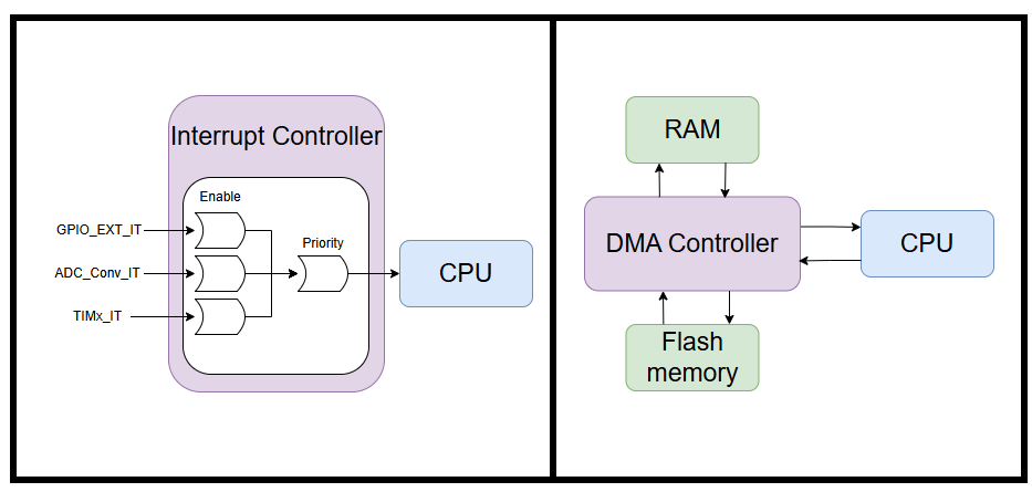
ADC with interrupts
Those were the most common ADC operation modes and might be required as you experience a single conversion mode is inefficient. What about ADC with interrupts? Can we just use them togeter such that ADC runs in the background and gives us a heads-up when the conversion is completed? It is very well possible!
When an ADC conversion completes, it can generate an interrupt. This is a common and efficient way to handle single or occasional ADC readings without constantly polling (repeatedly checking) a status flag in your main loop.
How it works:
- Configure ADC: Set up the ADC for the desired mode (single, continuous, scan, etc.), channel, sampling time, and resolution.
- Enable Interrupt: Enable the “End of Conversion” (EOC) interrupt for regular conversions (or “End of Injected Conversion” (JEOC) for injected conversions) within the ADC peripheral. You also need to enable the corresponding ADC interrupt in the Nested Vectored Interrupt Controller (NVIC).
- Start Conversion: Initiate an ADC conversion (either by software or a hardware trigger).
- CPU Continues: The CPU is free to execute other tasks while the ADC performs the conversion in the background.
- Interrupt Trigger: Once the ADC conversion is complete, the EOC (or JEOC) flag is set, and an interrupt request is generated.
- Interrupt Service Routine (ISR): The CPU jumps to the predefined ADC Interrupt Service Routine (ISR). Inside this ISR, you read the converted value from the ADC Data Register (ADC_DR) and clear the interrupt flag.
- CPU Resumes: After executing the ISR, the CPU returns to where it was interrupted in the main program.
One possible disadvantage of using ADC with interrupts might be overhead for high rates. If you need to acquire data very frequently (e.g., in continuous or high-speed scan modes), generating an interrupt for every single conversion (or even every sequence of conversions) can lead to significant CPU overhead. The CPU spends a lot of time entering and exiting the ISR, which can impact performance and introduce jitter.
ADC with DMA
DMA stands for “Direct Memory Access.” Imagine you want to move a lot of books from one shelf to another. Normally, you (the CPU) would have to pick up each book and carry it over, one by one, which takes a lot of your time. But if you have a helper (DMA), you can just tell them what to move and where, and they do it for you while you do something else.
In microcontrollers, DMA allows data to be transferred between memory and peripherals (like the DAC or ADC) automatically, without the CPU having to handle every single piece of data. This makes things much faster and frees up the CPU to do other tasks. In this exercise, DMA will send the sine wave data to the DAC automatically, so the microcontroller doesn’t have to send each value one by one.
This is incredibly powerful for high-speed or continuous data acquisition.
Details about the DMA setting are not in the scope of this course. It is just that you should know what DMA is and how to set up simple DMA with ADC and DAC applications. But if you want to learn more about the details of the settings, you can follow this link, but it will probably make more sense after you learn about DAC.
How it works: Configure ADC: Set up the ADC for continuous conversion, scan mode, or any mode where multiple conversions will occur.
Select DMA Stream and Channel: The STM32F767 has multiple DMA controllers (DMA1, DMA2), each with several “streams.” Each stream can be connected to a specific peripheral request (e.g., ADC1, ADC2, ADC3). You need to select the correct DMA stream and channel that corresponds to your ADC.
DMA vs Interrupt
| Scenario | DMA | Interrupt |
|---|---|---|
| Multi-channel at high speed | ✅ Efficient, handles easily | ⚠️ CPU load increases, ISR stack grows |
| Single Channel at low speed | ⚠️ Overkill | ✅ Simple and effective |
| Real-time control loop (e.g., PID) | ✅ Precise timing with Timer + DMA | ⚠️ ISR jitter may affect stability |
(Source: blog.embeddedexpert.io)
So with DMA, you can modify the memory without using CPU cycles at all!
Exercise: ADC single-continuous mode with interrupt
To start, you can either do changes on your previous project or create a new one and do the necessary pinout & clock configurations. I will explain the steps on top of the first ADC exercis here.
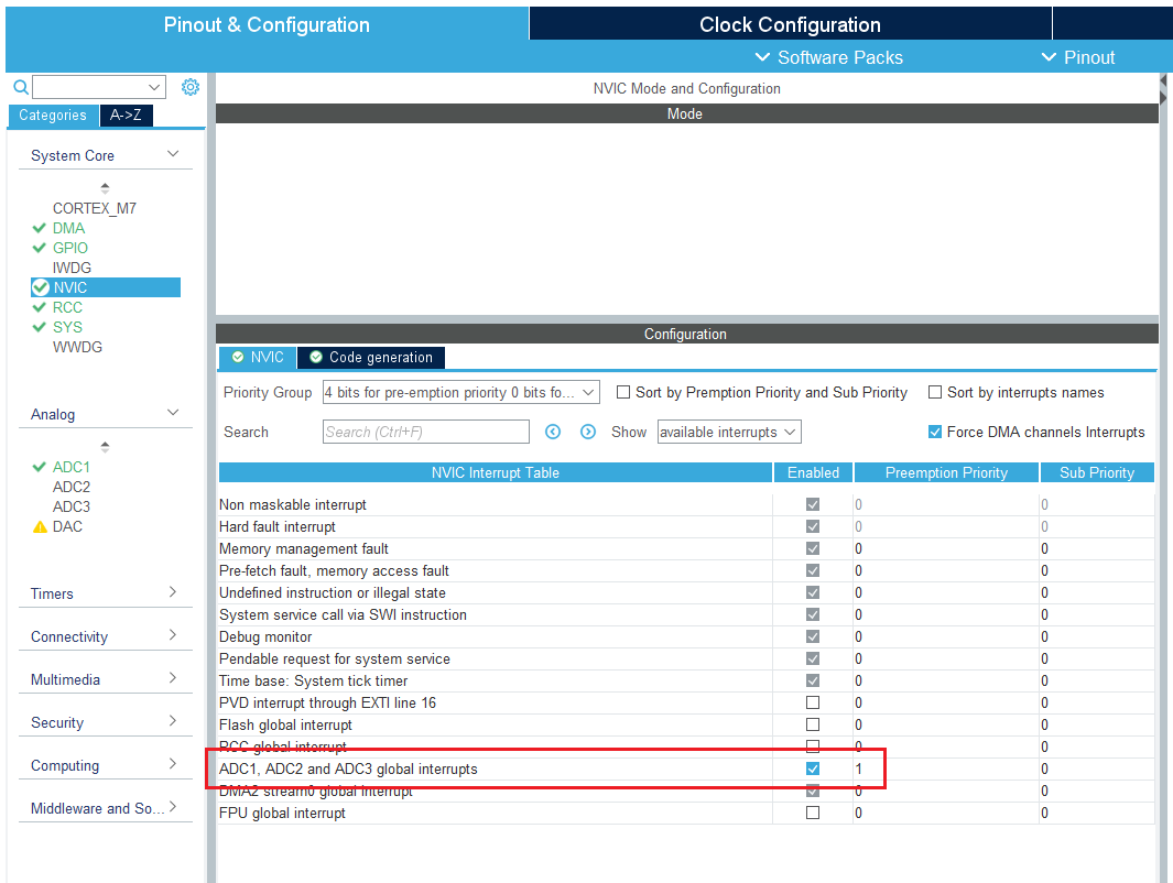
- Set the interrupts for ADC1:
ADC1 > Configuration > NVIC Settings > ADC1, ADC2 and ADC3 global interrupts : Enabled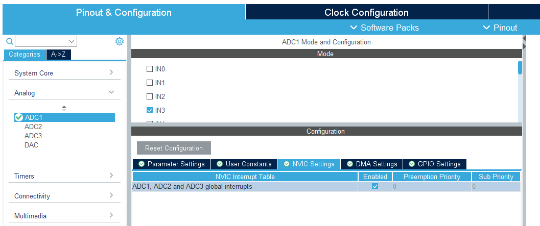
- Set the continuous mode enabled since we don’t want to call
HAL_ADC_Start(&hadc1);everytime a conversion is completed:ADC1 > Configuration > Parameter Settings > ADC_Settings > Scan Conversion Mode: Enabled,Continuous Conversion Mode: Enabled,End of Conversion Selection: EOC flag at the end of all conversions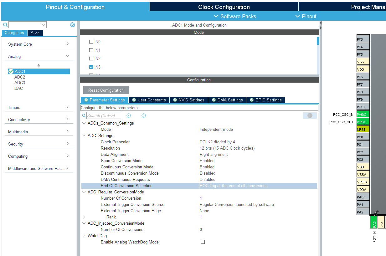
- Keep the clock configurations the same: 8 MHz input frequency and HCLK 108 Mhz.
- Give a proper name to your project. Do the necessary changes and generate your code.
- Create a platformio.ini with the previous content.
- Since the interrupt function needs access to some of the variables, we will move them from inside the
/* USER CODE BEGIN 1 */to inside to/* USER CODE BEGIN 0 */inmain.cwithvolatilekeyword.volatile uint32_t adc_value = 0; volatile float voltage = 0.0; uint16_t count = 0; - Make sure that you remove the variables in
/* USER CODE BEGIN 1 */. - Now we will start the ADC in interrupt mode. This will be before our infinite loop. Place this after
/* USER CODE BEGIN 2 */:HAL_ADC_Start_IT(&hadc1); - Let’s see which callback is called after this interrupt is completed. Ctrl + Click on the
HAL_ADC_Start_IT(), which will take you instm32f7xx_hal_adc.c. If you search “callback” in this file, you will see thathadc->ConvCpltCallback = HAL_ADC_ConvCpltCallback;in theHAL_ADC_Init()function. Perfect! Like in other callbacks, this is also a weak function, whick means that we can implement our own version inmain.c. Place this code after/* USER CODE BEGIN 4 */:void HAL_ADC_ConvCpltCallback(ADC_HandleTypeDef* hadc){ adc_value = HAL_ADC_GetValue(hadc); // Get the converted value // Convert ADC value to voltage // V_ref is 3.3V and 12-bit resolution (4096 levels) voltage = (float)adc_value * (3.3f / 4095.0f); } - Also, I want to add a counter variable to see the steps in our
int main(). Update the code after/* USER CODE BEGIN 3 */. Pay attention that we are not doing and ADC in the main function:count++; HAL_Delay(500); - Build and upload.
- Observe
count,adc_valueandvoltagein debugger’s watchlist.
Exercise: ADC Multi-channel with DMA
In this exercise, we will have more than one inputs in our ADC. In fact, we don’t have to use DMA as soon as we connect more than one analog input, but it is a much more efficient way to handle multi-channel ADC with DMA.
DMA (Direct Memory Access) is a hardware feature that allows certain peripherals to directly read from or write to memory without requiring constant intervention from the CPU.
To start, you can either do changes on your previous project or create a new one and do the necessary pinout & clock configurations. I will explain the steps on top of the first ADC exercis here.
- Add an LDR or a temperature sensor, or another potentiometer to your existing circuit and connect it to
PA4.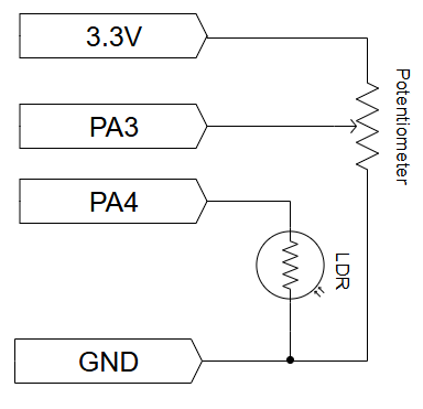
- Find
PA4on the chip and set it toADC1_IN4. Change the label toLDR_IN. - Change these in ADC1 Parameter Settings:
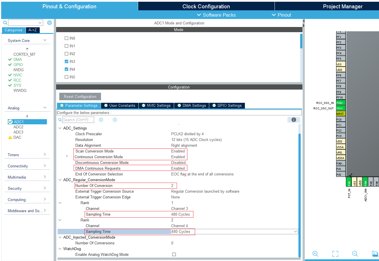 We want high sampling rate because we don’t want to stuck at the callback constantly. Also higher sampling rate means better accuracy in ADC.
 - Go to ADC1 DMA Settings:
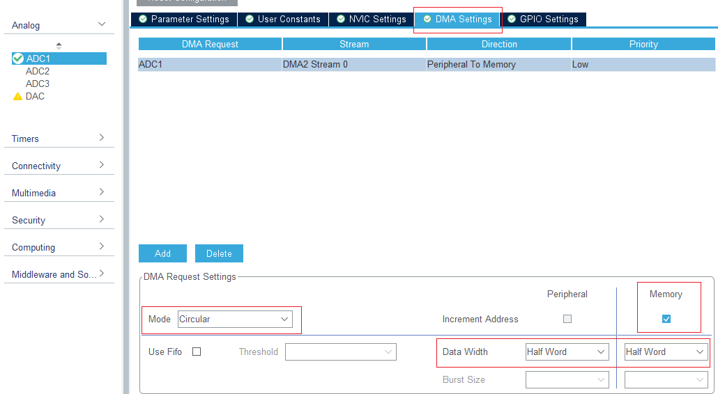 The meaning of continuous modes:
- ContinuousConvMode (ADC): “Hey ADC, keep converting non-stop!”
- DMAContinuousRequests (ADC): “Hey ADC, every time you have new data, tell the DMA to come get it!”
When all three are in sync (ContinuousConvMode = ENABLE, DMAContinuousRequests = ENABLE, and DMA Stream Mode = Circular), you achieve a very efficient, hands-off continuous data stream from the ADC to your memory buffer. The CPU only needs to process the data in the buffer when it’s ready.
- Adjust the NVIC settings on the left:
- Keep the clock configurations the same: 8 MHz input frequency and HCLK 108 Mhz.
- Give a proper name to your project. Do the necessary changes and generate your code.
- Create a platformio.ini with the previous content.
- (Optional) I want to define a bool flag for debugging. That’s why I include the
stdbool.hlibrary at the beginning where/* USER CODE BEGIN Includes */:# include <stdbool.h> - Here are our variables which will be placed after ``:
float pot_adc_volt = 0; float ldr_adc_volt = 0; volatile uint16_t pot_adc_val = 0; volatile uint16_t ldr_adc_val = 0; volatile uint16_t raw_adc_vals[2]; volatile bool conv_completed = false; uint16_t count = 0; - This time we will start the ADC in DMA mode. This will be before our infinite loop. Place this after
/* USER CODE BEGIN 2 */:HAL_ADC_Start_DMA(&hadc1, (uint32_t*)raw_adc_vals, 2); - Our main loop is like this. You can do whatever you want with the values, this is just for demo. The
countvariable is only for debugging.count++; if(conv_completed){ // Do whatever calculations/actions you want to do with the ADC readings pot_adc_volt = (float)pot_adc_val * (3.3f / 4095.0f); ldr_adc_volt = (float)ldr_adc_val * (3.3f / 4095.0f); conv_completed = false; } HAL_Delay(5); - In our
HAL_ADC_ConvCpltCallback()which we define after/* USER CODE BEGIN 4 */, we might skip doing anything there.raw_adc_valswill be updated periodically anyways. We could have used it as it is in our main loop without assigning to any other variable.void HAL_ADC_ConvCpltCallback(ADC_HandleTypeDef* hadc){ ldr_adc_val = raw_adc_vals[0]; pot_adc_val = raw_adc_vals[1]; conv_completed = true; // __NOP(); // Only for debugging to check if the callback is triggered correctly. It is like "pass" keyword in Python. } - Build and upload.
- Observe
countandraw_adc_valsin debugger’s watchlist.
If your debugger does not increment count properly, it might be about your stack size. More about stack overflows and increasing stack size
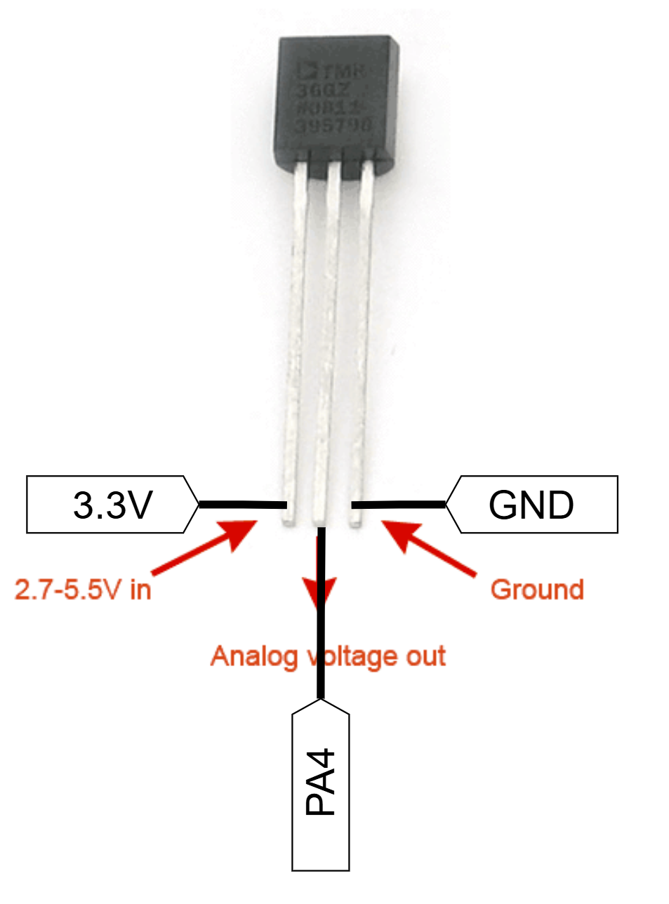
Exercise: Temperature sensor TMP36(Home/Lab)
In this example we will be reading the temperature from the TMP36 sensor that is included in the kit. The TMP36 has a voltage output linearly proportional to the temperature, and thus makes it easy to measure temperatures without any curve fitting that must be used with nonlinear sensing elements.
The details of how the TMP36 operates are available in the datasheet
Connect the sensor according to the following diagram:
The rest is in your Assignment-3 :)